last edited: 2026-06-05 09:06:10 +0000
The gem5 Memory System
The document describes memory subsystem in gem5 with focus on program flow during CPU’s simple memory transactions (read or write).
Model Hierarchy
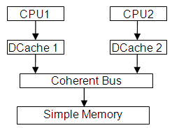
Model that is used in this document consists of two out-of-order (O3) ARM v7 CPUs with corresponding L1 data caches and Simple Memory. It is created by running gem5 with the following parameters:
configs/example/fs.py –-caches –-cpu-type=arm_detailed –-num-cpus=2
Gem5 uses Simulation Objects derived objects as basic blocks for building memory system. They are connected via ports with established master/slave hierarchy. Data flow is initiated on master port while the response messages and snoop queries appear on the slave port.
CPU
Data Cache object implements a standard cache structure:
It is not in the scope of this document to describe O3 CPU model in details, so here are only a few relevant notes about the model:
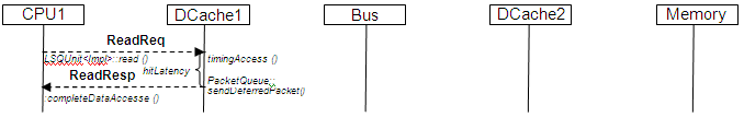
Read access is initiated by sending message to the port towards DCache object. If DCache rejects the message (for being blocked or busy) CPU will flush the pipeline and the access will be re-attempted later on. The access is completed upon receiving reply message (ReadRep) from DCache.
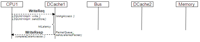
Write access is initiated by storing the request into store buffer whose context is emptied and sent to DCache on every tick. DCache may also reject the request. Write access is completed when write reply (WriteRep) message is received from DCache.
Load & store buffers (for read and write access) don’t impose any restriction on the number of active memory accesses. Therefore, the maximum number of outstanding CPU’s memory access requests is not limited by CPU Simulation Object but by underlying memory system model.
Split memory access is implemented.
The message that is sent by CPU contains memory type (Normal, Device, Strongly Ordered and cachebility) of the accessed region. However, this is not being used by the rest of the model that takes more simplified approach towards memory types.
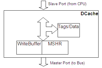
Data Cache Object
Data Cache object implements a standard cache structure:
Cached memory reads that match particular cache tag (with Valid & Read flags) will be completed (by sending ReadResp to CPU) after a configurable time. Otherwise, the request is forwarded to Miss Status and Handling Register (MSHR) block.
Cached memory writes that match particular cache tag (with Valid, Read & Write flags) will be completed (by sending WriteResp CPU) after the same configurable time. Otherwise, the request is forwarded to Miss Status and Handling Register(MSHR) block.
Uncached memory reads are forwarded to MSHR block.
Uncached memory writes are forwarded to WriteBuffer block.
Evicted (& dirty) cache lines are forwarded to WriteBuffer block.
CPU’s access to Data Cache is blocked if any of the following is true:
- MSHR block is full. (The size of MSHR’s buffer is configurable.)
- Writeback block is full. (The size of the block’s buffer is configurable.)
- The number of outstanding memory accesses against the same memory cache line has reached configurable threshold value – see MSHR and Write Buffer for details.
Data Cache in block state will reject any request from slave port (from CPU) regardless of whether it would result in cache hit or miss. Note that incoming messages on master port (response messages and snoop requests) are never rejected.
Cache hit on uncachable memory region (unpredicted behaviour according to ARM ARM) will invalidate cache line and fetch data from memory.
Tags & Data Block
Cache lines (referred as blocks in source code) are organised into sets with configurable associativity and size. They have the following status flags:
- Valid. It holds data. Address tag is valid
- Read. No read request will be accepted without this flag being set. For example, cache line is valid and unreadable when it waits for write flag to complete write access.
- Write. It may accept writes. Cache line with Write flags identifies Unique state – no other cache memory holds the copy.
- Dirty. It needs Writeback when evicted.
Read access will hit cache line if address tags match and Valid and Read flags are set. Write access will hit cache line if address tags match and Valid, Read and Write flags are set.
MSHR and Write Buffer Queues
Miss Status and Handling Register (MSHR) queue holds the list of CPU’s outstanding memory requests that require read access to lower memory level. They are:
- Cached Read misses.
- Cached Write misses.
- Uncached reads.
WriteBuffer queue holds the following memory requests:
- Uncached writes.
- Writeback from evicted (& dirty) cache lines.
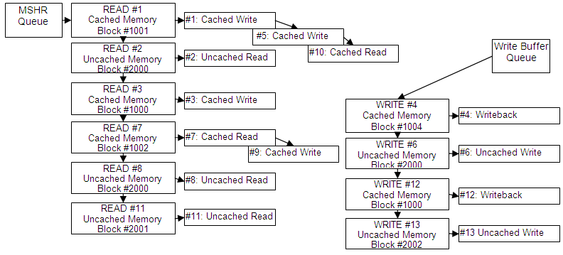
Each memory request is assigned to corresponding MSHR object (READ or WRITE on diagram above) that represents particular block (cache line) of memory that has to be read or written in order to complete the command(s). As shown on gigure above, cached read/writes against the same cache line have a common MSHR object and will be completed with a single memory access.
The size of the block (and therefore the size of read/write access to lower memory) is:
- The size of cache line for cached access & writeback;
- As specified in CPU instruction for uncached access.
In general, Data Cache model distinguishes between just two memory types:
- Normal Cached memory. It is always treated as write back, read and write allocate.
- Normal uncached, Device and Strongly Ordered types are treated equally (as uncached memory)
Memory Access Ordering
An unique order number is assigned to each CPU read/write request(as they appear on slave port). Order numbers of MSHR objects are copied from the first assigned read/write.
Memory read/writes from each of these two queues are executed in order (according to the assigned order number). When both queues are not empty the model will execute memory read from MSHR block unless WriteBuffer is full. It will, however, always preserve the order of read/writes on the same (or overlapping) memory cache line (block).
In summary:
- Order of accesses to cached memory is not preserved unless they target the same cache line. For example, the accesses #1, #5 & #10 will complete simultaneously in the same tick (still in order). The access #5 will complete before #3.
- Order of all uncached memory writes is preserved. Write#6 always completes before Write#13.
- Order to all uncached memory reads is preserved. Read#2 always completes before Read#8.
- The order of a read and a write uncached access is not necessarily preserved unless their access regions overlap. Therefore, Write#6 always completes before Read#8 (they target the same memory block). However, Write#13 may complete before Read#8.
Coherent Bus Object
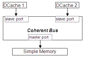
Coherent Bus object provides basic support for snoop protocol:
All requests on the slave port are forwarded to the appropriate master port. Requests for cached memory regions are also forwarded to other slave ports (as snoop requests).
Master port replies are forwarded to the appropriate slave port.
Master port snoop requests are forwarded to all slave ports.
Slave port snoop replies are forwarded to the port that was the source of the request. (Note that the source of snoop request can be either slave or master port.)
The bus declares itself blocked for a configurable period of time after any of the following events:
- A packet is sent (or failed to be sent) to a slave port.
- A reply message is sent to a master port.
- Snoop response from one slave port is sent to another slave port.
The bus in blocked state rejects the following incoming messages:
- Slave port requests.
- Master port replies.
- Master port snoop requests.
Simple Memory Object
It never blocks the access on slave port.
Memory read/write takes immediate effect. (Read or write is performed when the request is received).
Reply message is sent after a configurable period of time .
Message Flow
Memory Access Ordering
The following diagram shows read access that hits Data Cache line with Valid and Read flags:
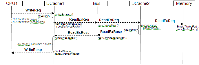
Cache miss read access will generate the following sequence of messages:
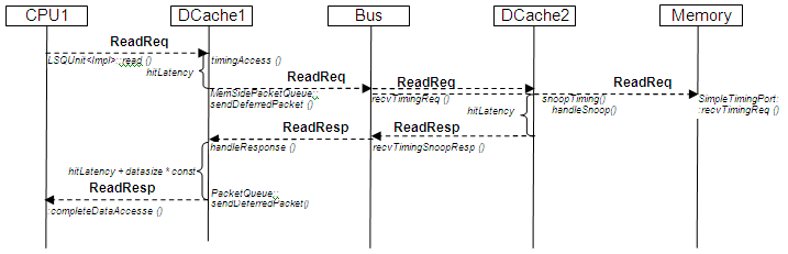
Note that bus object never gets response from both DCache2 and Memory object. It sends the very same ReadReq package (message) object to memory and data cache. When Data Cache wants to reply on snoop request it marks the message with MEM_INHIBIT flag that tells Memory object not to process the message.
Memory Access Ordering
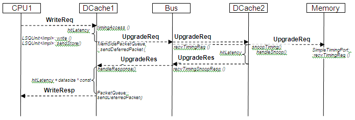
The following diagram shows write access that hits DCache1 cache line with Valid & Write flags:
Next figure shows write access that hits DCache1 cache line with Valid but no Write flags – which qualifies as write miss. DCache1 issues UpgradeReq to obtain write permission. DCache2::snoopTiming will invalidate cache line that has been hit. Note that UpgradeResp message doesn’t carry data.
The next diagram shows write miss in DCache. ReadExReq invalidates cache line in DCache2. ReadExResp carries the content of memory cache line.